Product Overview Product Overview
..................................................
Wafer Bumping
..................................................
Wafer Level CSP
..................................................
BGA/LGA
..................................................
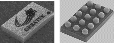
Flip Chip CSP
..................................................
QFN/DFN
..................................................
Flip Chip QFN/DFN/SOP/TSOT
..................................................
P-DIP
..................................................
TO&SOT
..................................................
SOIC / SSOP / TSSOP
..................................................
SOJ&PLCC
..................................................
QFP / LQFP / TQFP |